
Requirements & design
Define the intended application and the electrical, thermal, package and interface requirements that guide development.
Products
Application-led wafer and device design capability.
Part of GaN Technology.
Bryantech combines system architecture, electronic design, embedded intelligence, verification and production thinking to shape a dependable solution.
Detailed specifications, availability and programme-specific compliance information are confirmed with our engineering team before engagement.
Discuss this solution ↗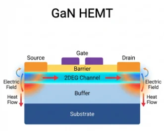
Engineering in practice
Bryantech supports GaN HEMT programmes through requirements, design interfaces, fabrication coordination and validation. Device and process work is coordinated with the specialist resources required by the programme.
Applications
Power conversion and custom electronic systems using GaN technology.
Technical scope tailored to your system and development stage.
Define the intended application and the electrical, thermal, package and interface requirements that guide development.
Coordinate device-design and fabrication-process interfaces with the selected manufacturing partners.
Plan sample builds and the documentation needed to connect fabrication activity with engineering evaluation.
Agree test conditions, organize evaluation results and feed findings back into the development process.
A structured sequence with review points and recorded decisions.
Agree device and application requirements.
Coordinate design and process interfaces.
Organize engineering builds.
Review results against agreed criteria.
The agreed package supports design review, integration and the next project stage.
Requirements, design-interface documentation and sample plans.
Evaluation plans, test documentation and engineering review actions.
Build what comes next